
cross-posted from: https://hexbear.net/post/621898
In this photo, you can see how much the on-die cache has expanded compared to its predecessors and other contemporary embedded microprocessors. Really foreshadowing the kind of optimizations that would become commonplace today. In addition to its very large (for the time) 4-way set associative 256kb on-die secondary cache, it featured a 16k primary instruction cache and 16k primary data cache. It was fabricated at a 250 nanometer feature size and could be clocked up to 263 MHz. With its dual-issue superscalar 5-stage pipeline, it could achieve a Dhrystone score of 450 DMIPS at 263 MHz, a impressive score for embedded microprocessors of the time, although this benchmark really doesn't show off its cache performance.
Anyway, hope you like the pretty die shot of this forgotten microprocessor.
It's a picture of the inside of a computer processor.
Here's a zoomed out version for scale:
Show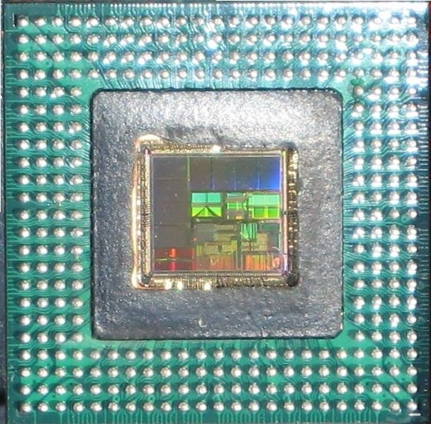

